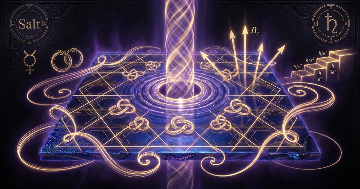
Quantum Hall Effect in Crystalline 2D Semiconductors
Mineral Classification & Crystallographic Thesis: Heterostructure Substrates Hosting the 2DEG
Epitaxial Interfaces: Zincblende GaAs/AlGaAs and Hexagonal Boron Nitride/Graphene
The physical realization of a high-mobility two-dimensional electron gas (2DEG) is fundamentally an exercise in precision mineralogy and solid-state synthesis. Far from existing as idealized, mathematical planes suspended in vacuum, 2DEGs depend strictly upon the sub-angstrom interfacial coherence of polar semiconductor matrices. Within molecular beam epitaxy (MBE) chambers, pristine interfaces are synthesized through the atomic layer-by-layer deposition of alternating compound crystals, most prominently the polar zincblende heterojunction formed by gallium arsenide ($\text{GaAs}$) and aluminum gallium arsenide ($\text{Al}{x}\text{Ga}{1-x}\text{As}$). The crystallographic fidelity of this boundary is dictated by the precise match of their respective cubic lattice parameters; at $x \approx 0.3$, the lattice parameter mismatch between $\text{GaAs}$ ($a = 5.6533\text{ \AA}$) and $\text{Al}{0.3}\text{Ga}{0.7}\text{As}$ ($a = 5.6574\text{ \AA}$) is less than $0.1%$, preventing the formation of misfit edge dislocations that would otherwise act as non-radiative scattering centers and catastrophic carrier traps.
Beyond cubic arsenides, the frontier of two-dimensional transport occupies the hexagonal system ($P6_3/mmc$), epitomized by the van der Waals assembly of exfoliated monolayer graphene positioned upon ultra-flat hexagonal boron nitride ($\text{hBN}$) substrates, as explored in /crystals-materials/graphene-hexagonal-boron-nitride-superlattices. In this laminar geometry, the boron nitride underlayer supplies a dielectrically uniform, atomically planar crystallographic pedestal that suppresses out-of-plane flexural phonons and eliminates localized dangling bonds. Because graphene’s honeycomb network of $sp^2$-hybridized carbon atoms exhibits an in-plane lattice constant of $a = 2.46\text{ \AA}$, while hexagonal boron nitride exhibits $a = 2.50\text{ \AA}$, a controlled rotational alignment yields long-wavelength moiré superlattices. These geometries fundamentally reshape the planar band structure into isolated, flat mini-bands, establishing the crystallographic architecture required to observe the fractional quantum Hall effect 2d electron gas crystals exhibit under pristine transport conditions.
+----------------------------------------------------------------------------------------------------+
| LATTICE MISMATCH AND DIELECTRIC PROPERTIES                                                        |
+----------------------+--------------------+---------------------+------------------+---------------+
| Heterostructure Host | Crystal System     | Space Group         | Lattice Mismatch | ε_r (at 4.2K) |
+----------------------+--------------------+---------------------+------------------+---------------+
| GaAs / Al_0.3Ga_0.7As| Cubic (Zincblende) | F-43m (No. 216)     | < 0.10 %         | 12.9          |
| Graphene / hBN       | Hexagonal (Laminar)| P6_3/mmc (No. 194)  | ~ 1.70 %         | 3.9           |
| InAs / AlGaSb        | Cubic (Zincblende) | F-43m (No. 216)     | ~ 0.65 %         | 15.2          |
+----------------------+--------------------+---------------------+------------------+---------------+Primary structural characteristics compiled from:
- von Klitzing, K., Dorda, G., & Pepper, M. (1980). New Method for High-Accuracy Determination of the Fine-Structure Constant Based on Quantized Hall Resistance. Physical Review Letters, 45(6), 494–497.
- Tsui, D. C., Stormer, H. L., & Gossard, A. C. (1982). Two-Dimensional Magnetotransport in the Extreme Quantum Limit. Physical Review Letters, 48(22), 1559–1562. Crystallographic indices: Zincblende $\text{GaAs}$ possesses a face-centered cubic lattice populated by dual interpenetrating FCC sublattices shifted by $(1/4, 1/4, 1/4)a$, with space group $F\bar{4}3m$ (No. 216). Low-temperature relative dielectric constant $\varepsilon_r \approx 12.9$; low-temperature electron mobilities exceed $\mu = 10^7\text{ cm}^2/\text{V}\cdot\text{s}$. Hexagonal Boron Nitride ($\text{hBN}$) crystallizes in the $P6_3/mmc$ (No. 194) space group with in-plane lattice constant $a = 2.504\text{ \AA}$ and out-of-plane $c = 6.660\text{ \AA}$, providing an electrically inert, atomically flat dielectric substrate ($\varepsilon_r \approx 3.9$).
Point-Group Symmetry and Cleavage Morphology of Semiconductor Hosts
The physical mechanics governing electron transport at these buried interfaces are directly linked to the underlying point-group symmetry of the host crystal. Zincblende semiconductors belong to the non-centrosymmetric cubic point group $\bar{4}3m$. Lacking an inversion center, these crystal matrices exhibit non-zero third-rank piezoelectric tensors ($d_{14} \neq 0$), yielding an intrinsic piezoelectricity that couples microscopic lattice strain directly to internal electric displacement fields. When an epitaxial layer is grown along the polar $[001]$ or $[111]$ crystallographic directions, interface strain manifests an internal polarization field. This field perturbs the electrostatic landscape of the quantum well, modulating the distribution of the electron gas and producing anisotropic spin splittings via the Dresselhaus spin-orbit interaction, which arises strictly from the bulk inversion asymmetry of the $\bar{4}3m$ crystal field.
The mechanical integrity of these heterostructures is mediated by classical crystallographic cleavage behavior. Zincblende crystals exhibit dominant cleavage along the ${110}$ planes, where neutral alternating rows of cations and anions minimize electrostatic surface energy during planar separation. This mineralogical property reflects an intermediate Mohs hardness ($\text{GaAs}$ exhibits a Mohs hardness of approximately $4.5$, in contrast to diamond-structure silicon at $7.0$), requiring strict handling protocols during substrate preparation and thinning.
The planar morphology of cleavage fragments dictates the boundary conditions of the synthesized Hall bar. Scattering from irregular micro-cleavage steps introduces boundary roughness, which dampens low-field Shubnikov–de Haas oscillations and accelerates the quantum decoherence of fractional phases. The preservation of singular, crystalline basal morphology is thus indispensable for observing non-Abelian quantum states.
[GaAs / AlGaAs Interfacial Matrix]
  │
  ├─► Space Group: F-43m (Cubic Zincblende)
  │     └─► Lacks structural inversion center
  │     └─► Activates non-zero piezoelectric tensor d_14
  │     └─► Generates intrinsic Dresselhaus spin-orbit field
  │
  └─► Primary Cleavage Habit: {110} Neutral Plane
        └─► Minimizes electrostatic dipole moments across the fracture interface
        └─► Governs atomic boundary smoothness required for ballistic edge channels
The Quantum Well Confinement Paradigm as an Engineered Mineral Matrix
Modulation doping, pioneered in crystalline semiconductor engineering, represents the deliberate restructuring of mineral chemistry to achieve spatial decoupling between mobile carriers and their parent ionic dopants. Silicon donors ($\text{Si}^{4+}$ substituting for $\text{Ga}^{3+}$ sites) are positioned exclusively within the $\text{Al}x\text{Ga}{1-x}\text{As}$ barrier, isolated from the active $\text{GaAs}$ transport channel by an undoped spacer layer spanning tens of nanometers. Electrons thermally ionize from these donors and transfer into the adjacent lower-conduction-band $\text{GaAs}$ matrix, pulled across the abrupt heterojunction by electrochemical potential alignment.
Conduction Band Energy Diagram (Modulation-Doped Interface):
Energy [eV]
▲
│      AlGaAs Barrier Layer            GaAs Channel Layer
│   (Contains Si Donor Ions)          (Ultra-Pure Matrix)
│
E_c│   ────────────────────────┐
│                           │
│                           │  Conduction Band Offset (ΔE_c ≈ 0.3 eV)
│                           └───┐
E_F│  - - - - - - - - - - - - - - -│- - - - - - - - - - - - - - - - -
│                                \     Triangular Well
│                                 \  ┌───────────────────────┐
│                                  _│ Quantum Confined 2DEG │
│                                    └───────────────────────┘
└──────────────────────────────────────────────────────────────────► Growth Axis z
This thermodynamic redistribution bends the conduction band edge, constructing a quasi-triangular electrostatic potential well bounded by the sharp band offset $\Delta E_c$ on the interfacial side and the electrostatic depletion field on the substrate side. The spatial dimensions of this well—typically less than $10\text{ nm}$ in breadth—are comparable to or smaller than the de Broglie wavelength of the mobile electrons. As a consequence, the continuous spectrum of out-of-plane momentum $k_z$ quantizes into discrete energy subbands:
$$E_n(k_x, k_y) = \mathcal{E}_n + \frac{\hbar^2 (k_x^2 + k_y^2)}{2m^*}$$
where $m^$ is the conduction-band effective mass ($m^ \approx 0.067,m_0$ in $\text{GaAs}$). At cryogenic temperatures ($T < 4.2\text{ K}$), only the lowest subband $\mathcal{E}_0$ is populated, reducing the phase space of the system to a strictly two-dimensional continuum.
This engineered mineral matrix suppresses ionized impurity scattering by orders of magnitude; the separation of the positive donor ions from the 2DEG ensures that carriers glide through the sub-angstrom crystalline lattice with mean free paths exceeding $10\text{ }\mu\text{m}$. The macroscopic dielectric constant of the surrounding medium ($\varepsilon_r \approx 12.9$) shields the remaining residual Coulomb fluctuations, allowing quantum-scale collective ground states to emerge unhindered by thermal and structural disorder.
Lattice Geometry & Solid-State Physics: Landau Levels Quantization and Chern Numbers
Orbital Degeneracy and Magnetic Length in Perpendicular Gauge Fields
When an intense, uniform magnetic field $\mathbf{B} = (0, 0, B_z)$ is applied perpendicular to the plane of an engineered 2DEG, the continuous two-dimensional parabolic dispersion relation of the conduction electrons collapses. The canonical momentum operator $\mathbf{P} = -i\hbar\boldsymbol{\nabla} + e\mathbf{A}$ governs the system, where $\mathbf{A}$ represents the electromagnetic vector potential. Adopting the Landau gauge $\mathbf{A} = (-B_z y, 0, 0)$, the single-particle Hamiltonian maps algebraically to a harmonic oscillator equation of motion:
$$\hat{H} = \frac{1}{2m^} \left( -i\hbar\frac{\partial}{\partial x} - e B_z y \right)^2 - \frac{\hbar^2}{2m^} \frac{\partial^2}{\partial y^2}$$
This Hamiltonian quenches the kinetic energy spectrum into discrete, highly degenerate eigenvalues denoted as Landau levels:
$$E_n = \left( n + \frac{1}{2} \right) \hbar \omega_c \pm \frac{1}{2} g^* \mu_B B_z$$
where $\omega_c = eB_z / m^$ signifies the cyclotron frequency, $n \in {0, 1, 2, \dots}$ is the orbital quantum number, $g^$ represents the effective Landé $g$-factor ($g^* \approx -0.44$ for bulk $\text{GaAs}$), and $\mu_B$ is the Bohr magneton.
Energy [E]
    ▲
    │                                                      E_2 = (5/2)ħω_c
    │   ================================================== Landau Level n = 2
    │                         ▲
    │                         │  Cyclotron Energy Gap (ħω_c)
    │                         ▼
    │   ================================================== Landau Level n = 1
    │                         ▲
    │                         │  Cyclotron Energy Gap (ħω_c)
    │                         ▼
    │   -------------------------------------------------- Fermi Level E_F (in bulk gap)
    │                         ▲
    │                         │  Zeeman Splitting (g* μ_B B)
    │                         ▼
    │   ================================================== Landau Level n = 0
    │
    └────────────────────────────────────────────────────────────────────────► Density of States
The intrinsic length scale governing these quantized harmonic orbits is the magnetic length:
$$\ell_B = \sqrt{\frac{\hbar}{e B_z}}$$
At a typical magnetic field of $B_z = 10\text{ Tesla}$, $\ell_B \approx 8.1\text{ nm}$, which is significantly larger than the underlying semiconductor unit cell parameter ($a \approx 0.56\text{ nm}$). This scale separation permits treatment of the electron dynamics within an effective-mass envelope approximation while remaining confined by the magnetic flux quantum $\Phi_0 = h/e$.
Each Landau level possesses a macroscopic orbital degeneracy per unit area given by:
$$N_L = \frac{B_z}{\Phi_0} = \frac{e B_z}{h}$$
When accounting for spin degeneracy, this macroscopically degenerate manifold acts as an ultra-dense array of localized quantum orbitals, setting the stage for macro-coherent topological order.
Topological Chern Invariants and Incompressible Laughlin Fluids
The mathematical foundation of the integer quantum Hall effect (IQHE) is anchored in the topological invariant of the electronic ground state, rigorously formulated by Thouless, Kohmoto, Nightingale, and den Nijs (TKNN, 1982). Within a periodic crystalline potential subject to a rational magnetic flux per unit cell, the single-particle Bloch wavefunctions acquire a geometric structure characterized by the Berry connection:
$$\mathbf{A}n(\mathbf{k}) = i \langle u_n(\mathbf{k}) | \boldsymbol{\nabla}{\mathbf{k}} | u_n(\mathbf{k}) \rangle$$
The integral of the corresponding Berry curvature $\mathbf{\Omega}n(\mathbf{k}) = \boldsymbol{\nabla}{\mathbf{k}} \times \mathbf{A}_n(\mathbf{k})$ over the closed two-dimensional magnetic Brillouin zone (MBZ) yields an invariant integer, the first Chern class $\mathcal{C}_n$:
$$\mathcal{C}n = \frac{1}{2\pi} \int{\text{MBZ}} \mathbf{\Omega}_n(\mathbf{k}) \cdot d^2\mathbf{k} \quad (\mathcal{C}_n \in \mathbb{Z})$$
The total Hall conductivity $\sigma_{xy}$ of the system is the sum of these Chern numbers over all fully occupied Landau subbands beneath the Fermi energy:
$$\sigma_{xy} = \frac{e^2}{h} \sum_{n} \mathcal{C}_n = \nu \frac{e^2}{h}$$
where $\nu \in \mathbb{Z}$ represents the integer filling factor:
$$\nu = \frac{n_s}{N_L} = n_s \frac{h}{e B_z}$$
Because $\mathcal{C}_n$ is topologically invariant against smooth perturbations of the Hamiltonian, small concentrations of point defects, dislocations, or impurities in the semiconductor crystal cannot alter the Hall conductance; they merely localize states within the Landau level tails without perturbing the topological winding number.
Magnetic Brillouin Zone (MBZ) Topology:

       k_y ▲
           │      ┌───────────────────────────────┐
           │      │   / / / / / / / / / / / / /   │
           │      │ / / /  Berry Curvature  / / / │   Closed Torus Integration:
           │      │/ / /    Ω_n(k) Flux    / / /  │
           │      │ / / / / / / / / / / / / / /   │   C_n = (1/2π) ∬ Ω_n(k) d²k
           │      │/ / / / / / / / / / / / / / /  │       = Quantized Integer
           │      └───────────────────────────────┘
           └──────────────────────────────────────► k_x
In the extreme quantum limit, where the lowest Landau level ($n=0$) is only partially filled ($\nu < 1$), the single-particle kinetic energy is quenched, and electron-electron Coulomb interactions dominate the Hamiltonian. Tsui, Stormer, and Gossard (1982) discovered that at rational fractional filling factors with odd denominators—such as $\nu = 1/3$ and $\nu = 2/5$—the electron gas condenses into a correlated, incompressible quantum liquid. Laughlin (1983) constructed the variational many-body wavefunction describing this state at $\nu = 1/m$ (where $m$ is an odd integer for fermions):
$$\Psi_m(z_1, z_2, \dots, z_N) = \prod_{j < k}^N (z_j - z_k)^m \exp\left( -\frac{1}{4\ell_B^2} \sum_{i=1}^N |z_i|^2 \right)$$
Here, $z_j = x_j - i y_j$ denotes the complex spatial coordinates of the $j$-th electron. The fundamental Jastrow polynomial factor $(z_j - z_k)^m$ enforces a high-order zero whenever two electrons approach one another, minimizing the intra-plane Coulomb repulsion energy far more effectively than any classical charge distribution or mean-field approximation.
Because the exponent $m$ is an odd integer, the wavefunction satisfies the antisymmetry required by Fermi-Dirac statistics under particle exchange. The incompressibility of this Laughlin state means that creating a localized volume compression requires overcoming an excitation gap $\Delta \sim e^2 / (\varepsilon_r \ell_B)$. The elementary excitations of this correlated fluid are not ordinary electrons, but emergent vortices carrying fractional elementary charge $e^* = \pm e/m$ and fractional, anyonic braiding statistics.
Fractional Filling Factors and Composite Fermion Formulations
The fractional quantum Hall effect (FQHE) is unified and generalized by Jain’s composite fermion (CF) theory. Under strong magnetic fields and intense Coulomb repulsion, an electron binds to an even number $2p$ of quantum magnetic flux vortices ($\phi_0 = h/e$). This combined entity—an electron merged with an artificial gauge field—is a composite fermion:
$$\Psi_{\text{CF}} = \mathcal{P}{\text{LLL}} \prod{j < k} (z_j - z_k)^{2p} \Psi_{\text{electrons}}$$
where $\mathcal{P}_{\text{LLL}}$ projects the collective state onto the lowest Landau level.
Electron-Vortex Fusion (Composite Fermion Construction):

       Bare Electron                 Flux Attachment                   Composite Fermion
     (Coulomb Repulsion)           (Even Gauge Vortices)          (Effective Low-Field Fermion)
             ●               +            (Φ₀) (Φ₀)           =             (●)
         e- charge                    2p Flux Quanta                     Quasiparticle
                                                                      experiences B* = B - 2p ρ Φ₀
These emergent composite fermions experience an effective, reduced magnetic field:
$$B^* = B - 2p \rho \Phi_0 = B - 2p n_s \frac{h}{e}$$
Consequently, the fractional quantum Hall effect of strongly interacting electrons mapping to a fractional filling factor $\nu$ can be treated as the integer quantum Hall effect of weakly interacting composite fermions occupying non-interacting effective Landau levels (called $\Lambda$-levels), characterized by an integer filling factor $p^*$:
$$\nu = \frac{p^}{2p p^ \pm 1}$$
For instance, when $p=1$ and $p^=1$, this relation produces $\nu = 1/3$. When $p=1$ and $p^=2$, it yields $\nu = 2/5$. At exactly $\nu = 1/2$, the external magnetic field is fully cancelled by the attached statistical gauge flux ($B^* = 0$). In this regime, the composite fermions form a compressible Fermi liquid with a defined Fermi surface in zero effective field, explaining the absence of a Hall plateau at $\nu = 1/2$ despite strong external magnetic fields.
At the special fractional filling factor $\nu = 5/2$ within the second Landau level ($n=1$), pairing between composite fermions produces the Moore-Read Pfaffian state, which supports non-Abelian anyonic excitations whose exchange operations perform unitary topological rotations in a degenerate ground-state manifold.
Subtle Energetic Dynamics & Resonance Mechanics: Chiral Edge Modes and Zero-Point Coupling
Dissipationless 1D Edge Channels and Chiral Boundary Current Geometries
A consequence of non-trivial bulk topological order is the bulk-boundary correspondence: while the interior of a quantum Hall semiconductor is an electrical insulator with a finite energy gap to all charge excitations, the real-space physical perimeter hosts gapless, one-dimensional chiral edge states. Electrostatic confinement at the crystal perimeter forces the self-consistent potential $V(y)$ to curve upward toward the boundary. This confining potential shifts the energy of the Landau levels upward, causing them to intersect the Fermi energy $E_F$ and giving rise to localized conducting channels.
Cross-Section of Confined 2DEG (Spatial Potential vs. Energy):

  Energy [E]
      ▲
      │    Left Chiral Edge Mode                              Right Chiral Edge Mode
      │    Velocity: v_d = -(1/eB)∇V                          Velocity: v_d = +(1/eB)∇V
      │       \                                                      /
      │        \            Confinement Potential V(y)              /
      │         \                  ┌───────────┐                   /
      │          \                 │ BULK GAP  │                  /
   E_F│───────────\────────────────│(INSULATOR)│─────────────────/───────────
      │            \               └───────────┘                /
      │             \                                          /
      │              \________________________________________/
      │                         Landau Level n = 0
      └──────────────────────────────────────────────────────────────────────► Spatial Coordinate y
            y = 0 (Left Boundary)                             y = W (Right Boundary)
The semiclassical drift velocity of electrons occupying these boundary states is determined by the transverse gradient of the confining potential:
$$v_{\text{drift}} = \frac{1}{e B_z} \frac{\partial V(y)}{\partial y} \hat{\mathbf{x}}$$
Because the potential gradient $\partial V / \partial y$ has opposite signs at opposing boundaries of the Hall bar, the corresponding velocities have opposite signs: electrons on one edge travel in the $+\hat{\mathbf{x}}$ direction, while electrons on the opposite edge travel in the $-\hat{\mathbf{x}}$ direction.
These 1D edge states are strictly chiral. Elastic backscattering requires an incoming electron with wavevector $+k_x$ to transition into a state with wavevector $-k_x$. However, state with $-k_x$ does not exist on the same physical boundary; it is spatially isolated on the opposite side of the macroscopic crystal, separated by a bulk insulating barrier that spans millimeters. Consequently, the backward scattering matrix element vanishes exponentially:
$$\mathcal{M}_{\text{backscatter}} \sim \exp\left(-\frac{W}{\ell_B}\right) \to 0$$
where $W$ is the device width. Transport along the boundary is therefore dissipationless, yielding an exact longitudinal resistance $R_{xx} = 0$.
Quantum Bulk Insulator
- Charge excitations are pinned behind a thermodynamic energy gap: $\Delta = \hbar \omega_c$ (Integer) or $\Delta \sim e^2 / (\varepsilon_r \ell_B)$ (Fractional).
- Bulk longitudinal conductivity drops to zero ($\sigma_{xx} \to 0$) as $T \to 0\text{ K}$, mimicking an ideal dielectric.
- Displays zero-divergence orbital currents that cancel across adjacent magnetic cyclotron orbits.
- The bulk ground state is incompressible, supporting an invariant macroscopic topological order characterized by the Chern number $\mathcal{C}$.
Topological Chiral Edge Mode
- Gapless 1D boundary channels intersecting the chemical potential $E_F$ precisely at the crystal perimeters.
- Supports uninhibited ballistic transport where the longitudinal resistance drops to zero ($R_{xx} \to 0$).
- Backscattering is structurally forbidden by macroscopic spatial separation ($W \gg \ell_B$) and unidirectional chirality.
- Acts as a quantum-coherent perimeter current loop generating localized orbital magnetic moments coupled to boundary geometry.
Vacuum Polarization and Geometric Berry Phase Accumulation
The dynamics of the chiral edge state provide a direct laboratory window into geometric phases and quantum vacuum interactions. As a quasiparticle traverses the closed boundary perimeter $\mathcal{C}_{\text{perim}}$ of a quantum Hall device, its quantum state accumulates an adiabatic geometric phase—the Berry phase:
$$\gamma_B = \oint_{\mathcal{C}_{\text{perim}}} \mathbf{A}_R \cdot d\mathbf{R}$$
This phase shift operates identically to an Aharonov–Bohm phase induced by the magnetic flux enclosed by the real-space orbit, mapping microscopic orbital mechanics to macroscopic loop topology. These dynamics relate directly to the generalized formulations developed in /physics-electromagnetism/topological-insulators-berry-phase.
Under high magnetic fields, the physical boundary does not act merely as an electrostatic termination. Instead, it polarizes the local zero-point fluctuations of the surrounding electromagnetic field. The sharp spatial discontinuity in the dielectric constant between the high-index semiconductor matrix ($\varepsilon_r \approx 12.9$ for $\text{GaAs}$) and the external cryogenic vacuum ($\varepsilon_r = 1.0$) concentrates electric field gradients at the crystal boundary:
$$\mathbf{D}{\text{int}} \cdot \hat{\mathbf{n}} = \mathbf{D}{\text{ext}} \cdot \hat{\mathbf{n}}$$
This boundary matches the boundary equations of continuous quantum electrodynamics, turning the edge current loop into an ultra-low-noise quantum waveguide. It couples to geometric phases without the thermal and structural phase decoherence common to less ordered, non-topological conductors.
Resonance Coupling Between Quantum Hall Edge Currents and Subtle Bio-Informational Grids
The persistent, dissipationless perimeter current of a macroscopic quantum Hall bar creates an ultracoherent magnetic dipole and a non-divergent micro-torsional vector potential:
$$\mathbf{A}{\text{eff}}(\mathbf{r}) = \frac{\mu_0 I{\text{edge}}}{4\pi} \oint_{\mathcal{C}} \frac{d\mathbf{l}‘}{|\mathbf{r} - \mathbf{r}’|}$$
Because this chiral loop lacks the thermal and dissipative fluctuations typical of classical conductors ($R_{xx} = 0$), the phase noise of the generated vector potential approaches the fundamental quantum limit. In subtle energy paradigms, such macroscopic quantum loops are considered solid-state physical analogues to the organizing principles underlying biological meridians and cellular bio-informational arrays.
Subtle Field Interfacing:
[ Crystalline Boundary Geometry ] ──► [ Quantized Chiral Current Loop ]
                                                │
                                                ▼
                                   [ Phase-Coherent Vector Field A ]
                                                │
                                                ▼
                                   [ Zero-Point Geometric Resonance ]
                                                │
                                                ▼
                            [ Subtle Bio-Informational Coherence Coupling ]
Subtle energetic architectures rely upon geometric coherence and phase consistency to transfer informational patterns without thermal dissipation. When an engineered crystal hosts an active quantum Hall state, its perimeter acts as a physical boundary resonator. The macroscopic coherence factor:
$$\xi = \oint_{\mathcal{C}} \nabla \theta \cdot d\mathbf{l} = 2\pi n$$
stabilizes localized zero-point fluctuations into ordered geometries, showing how high-symmetry solid-state materials can bridge micro-scale quantum mechanics with larger informational fields.
Historical Lapidary Lore & Traditional Lineage: Planar Gemstones to Engineered Superlattices
Cleavage Planes in Classical Lapidary Traditions: From Muscovite to Specular Hematite
Long before the advent of ultra-high vacuum molecular beam epitaxy, early mineralogists recognized that certain natural crystal structures could be repeatedly cleaved into microscopically flat, thin sheets. Classical lapidary traditions focused extensively on phyllosilicates, most notably muscovite mica ($\text{KAl}_2(\text{AlSi}3\text{O}{10})(\text{OH})_2$), and laminar iron oxides like specular hematite ($\alpha\text{-Fe}_2\text{O}_3$). These minerals exhibit pronounced basal cleavage along the $(001)$ plane.
Natural phyllosilicates owe this macroscopic planar delamination to their fundamental microscopic architecture: continuous two-dimensional sheets of polymerized silicon-dioxide-tetrahedra ($\text{SiO}_4^{4-}$), interconnected by hexacoordinated aluminum octahedra and separated by weakly bound layers of univalent potassium ions ($\text{K}^+$). Lapidaries recognized that these sheets could be cleaved down to optical transparency, exhibiting uniform mechanical resistance and distinct dielectric isolation along their planes.
Classical Phyllosilicate Cleavage:
  ┌──────────────────────────────────────────────────────────────┐
  │ Tetrahedral Sheet (SiO_4 / AlO_4 Network)                    │  Strong Covalent/
  ├──────────────────────────────────────────────────────────────┤  Ionic In-Plane
  │ Octahedral Sheet (Al, Fe, Mg Core)                           │  Bonding
  ├──────────────────────────────────────────────────────────────┤
  │ Tetrahedral Sheet (SiO_4 / AlO_4 Network)                    │
  └──────────────────────────────────────────────────────────────┘
  ════════════════════════════════════════════════════════════════  Weak Interlayer
        K+ / Interlayer Cation Cleavage Plane (Basal 001)           Coulomb Bonds
  ════════════════════════════════════════════════════════════════  (Cleaves Easily)
  ┌──────────────────────────────────────────────────────────────┐
  │ Tetrahedral Sheet (SiO_4 / AlO_4 Network)                    │
  └──────────────────────────────────────────────────────────────┘
In ancient hermetic lapidaries, planar minerals showing basal cleavage were associated with shielding, reflective wards, and directional energy stabilization. Early practitioners observed that these stones were physically and thermally anisotropic—they cleaved along flat planes and resisted heat propagation along specific axes. This was interpreted as an innate capacity to redirect subtle forces along structured geometry.
Natural specular hematite, with its trigonal scalenohedral crystal habit ($\bar{3}2/m$), displays laminar, mirror-like plates that reflect light and conduct electricity anisotropically through its basal planes. The classical instinct to harness these planar minerals as protective and focusing tools anticipated the physics of two-dimensional confinement: constraining energy to an atomically flat plane fundamentally alters how it interacts with external fields.
Pliny and Theophrastus on Anisotropic Conduction and Laminated Stones
The mineralogical treatises of antiquity offer early recorded observations of directional anisotropy in laminated minerals. In De Lapidibus (c. 315 BCE), Theophrastus classified mineral specimens not merely by color, but by their mechanical response to cleavage, directional fracture, and their reaction to friction and heating. He documented that certain planar stones exhibited selective attraction when rubbed, an early recognition of the pyroelectric and piezoelectric behaviors typical of low-symmetry non-centrosymmetric crystals.
Centuries later, Pliny the Elder expanded these observations in his Naturalis Historia (Book 37), describing lapis specularis—a clear crystalline gypsum or mica that cleaved into thin, transparent sheets:
“Another stone is also found which may be split into as thin plates as the workman pleases; this stone, which is known as specularis, is found in Nearer Spain… It has the peculiarity of being composed of sheets which can be peeled off like layers of an onion, admitting the light and keeping out the weather, retaining within itself an immutable stillness.” — Pliny the Elder, Naturalis Historia, Book 37, Chapter 45.
Pliny’s description of lapis specularis focuses on its capacity to preserve an “immutable stillness” within, isolating the interior from external turbulence. Later medieval lapidaries, such as the Liber Lapidum of Marbode of Rennes (11th century), reinterpreted this observation through an esoteric lens, claiming that laminated, perfectly cleaved stones possessed an innate resistance to corruption, spiritual disturbances, and physical heat.
Viewed from modern solid-state physics, this lapidary lineage reflects an intuitive appreciation of the stability created by high-symmetry planar confinement. The geometric principles governing Platonic solid forms in nature, detailed in /sacred-geometry/platonic-solids-crystallography, show that macroscopic mineral order mirrors microscopic crystallographic symmetry. Modern 2D heterostructures, which isolate electron transport along pristine epitaxial planes, realize through solid-state engineering the directional stability and boundary isolation that early mineralogists intuited in naturally cleaved stones.
The Evolution of the Hall Effect: From Edwin Hall (1879) to von Klitzing’s Metrological Metamorphosis
The path to the quantum Hall effect began with the discovery of the classical Hall effect by Edwin H. Hall in 1879 at Johns Hopkins University. Working with thin gold leaves deposited on glass plates, Hall demonstrated that an applied magnetic field exerts a transverse Lorentz force on moving charge carriers:
$$\mathbf{F} = q(\mathbf{E} + \mathbf{v} \times \mathbf{B})$$
This transverse deflection builds up charge along the edges of the conductor until the resulting electrostatic Hall electric field balances the Lorentz force, yielding a continuous, linear transverse resistance:
$$R_{xy} = \frac{V_H}{I} = \frac{B_z}{n_s e}$$
Evolution of Hall Resistance Metrics:

Hall Resistance (R_xy)
   ▲
   │                                         Quantized Hall Plateaus (von Klitzing, 1980)
   │                                         R_H = h / (ν e²)
   │                                                  ┌───────────────
   │                                                  │ (ν = 1)
   │                                   ┌──────────────┘
   │                                   │ (ν = 2)
   │                    ┌──────────────┘
   │                    │ (ν = 3)
   │     - - - - - - - -│- - - - - - - - - - - Classical Hall Effect (Edwin Hall, 1879)
   │       / / / / / /  │                      R_xy ∝ B / n_s e (Linear Ramp)
   │     / / / / / / /  │
   │   / / / / / / / /  │
   │ / / / / / / / / /  │
   └────────────────────┴─────────────────────────────────────────────► Magnetic Field (B_z)
For over a century, the Hall effect was understood as a continuous diagnostic tool to measure charge carrier density $n_s$ and carrier polarity in bulk metals and doped semiconductors.
This continuous paradigm shifted in 1980, when Klaus von Klitzing, working with silicon metal-oxide-semiconductor field-effect transistors (MOSFETs) under high magnetic fields ($B > 10\text{ T}$) and liquid helium temperatures at the High Magnetic Field Laboratory in Grenoble, discovered that the transverse resistance does not scale continuously with magnetic field. Instead, it forms flat, invariant plateaus at quantized values:
$$R_H = \frac{h}{e^2 \nu}$$
where $\nu$ is an integer.
Simultaneously, the longitudinal resistance $R_{xx}$ drops to zero at each plateau, signaling the collapse of dissipation within the channel. This discovery transformed the Hall effect from a qualitative material diagnostic into an absolute, topologically protected constant of nature. The resistance standard h/e2, now known as the von Klitzing constant $R_K$:
$$R_K = \frac{h}{e^2} \approx 25812.80745\dots\ \Omega$$
freed electrical metrology from drift-prone physical artifacts, providing a direct anchor to Planck’s constant $h$ and the elementary charge $e$.
Practical Applications, Metrology & Handling Protocols: The Resistance Standard h/e^2
Primary Resistance Metrology: Realization of the von Klitzing Constant R_K
The primary modern application of the integer quantum Hall effect is in primary electrical metrology. Prior to the adoption of the revised SI system in 2019, national metrology institutes maintained the standard unit of electrical resistance (the ohm) through physical artifact standards, primarily wire-wound resistors constructed from manganin alloys. These artifacts suffered from resistance drift caused by mechanical strain, oxidation, and subtle temperature variations over time, requiring periodic cross-calibration against calculable capacitors.
SI Traceability Architecture (Post-2019 Revisions):
  [ Planck Constant h ] (Fixed Value)       [ Elementary Charge e ] (Fixed Value)
             │                                                │
             └───────────────────────┬────────────────────────┘
                                     ▼
                     [ von Klitzing Constant R_K = h/e² ]
                                     │
                                     ▼
               [ Cryogenic Quantum Hall Array Resistance Standard ]
                                     │
                                     ▼
                  [ Cryogenic Current Comparator (CCC) ]
                                     │
                                     ▼
               [ Primary Transfer Standards (100 Ω, 10 kΩ Resistors) ]</code></pre>
The realization of the quantized Hall resistance standard eliminates material drift entirely. Because the transverse resistance plateau at $\nu = 1$ is:
$$R_H(1) = R_K = \frac{h}{e^2} = 25812.8074593045\dots\ \Omega$$
the resistance is tied directly to fixed constants of nature.
Primary metrology laboratories combine quantum Hall resistance standards with Cryogenic Current Comparators (CCC). A CCC balances the ratio of currents traveling through a quantized Hall resistor and an adjustable decade resistor using an ultra-sensitive Superconducting Quantum Interference Device (SQUID) null detector. This system enables calibrations of secondary standard resistors (such as $100\text{ }\Omega$ or $10\text{ k}\Omega$ standards) with relative measurement uncertainties below $1 \times 10^{-9}$.
These setups interface directly with systems like /crystals-materials/piezoelectric-lattice-resonators, where high mechanical quality factors depend on low electrical dissipation and precise resistive calibrations.
Cryogenic and High-Field Instrumentation Protocols: Dilution Refrigerators and Superconducting Magnets
Observing and stabilizing the fractional quantum Hall effect 2d electron gas crystals exhibit requires extreme laboratory conditions:
- Thermal energy $k_B T$ must be reduced far below the excitation gap $\Delta$ of the correlated ground state. For fractional states, this gap is typically on the order of a few hundred millikelvin down to several millikelvin:
$$\Delta_{\nu} \sim \frac{C_{\nu} e^2}{4\pi \varepsilon_0 \varepsilon_r \ell_B} \ll \hbar \omega_c$$
- Operating temperatures must be maintained well below $50\text{ mK}$, often down to $5\text{–}10\text{ mK}$, using continuously operating helium-3/helium-4 ($^3\text{He}/^4\text{He}$) dilution refrigerators.
Dilution Refrigerator Instrumentation Topology:
±---------------------------------------------------------------+
| Room Temperature (300 K): RF-Shielded Lock-in / DAC Enclosure  |
±---------------------------------------------------------------+
│
High-Attenuation Thermocoax / Constantan Loom
│
±---------------------------------------------------------------+
| 4.2 K Stage: Main Helium Bath & Superconducting Solenoid (16 T)|
±---------------------------------------------------------------+
│
Sintered Silver Heat Exchangers
│
±---------------------------------------------------------------+
| Mixing Chamber (< 20 mK): Concentrated / Dilute ³He/⁴He Phase  |
|   ┌────────────────────────────────────────────────────────┐   |
|   │ Sample Cell: Sintered Silver Thermal Finger            │   |
|   │ Mounted GaAs/AlGaAs Hall Bar in Faraday Enclosure       │   |
|   └────────────────────────────────────────────────────────┘   |
±---------------------------------------------------------------+
- High magnetic fields are generated using superconducting solenoids wound from niobium-titanium ($\text{NbTi}$) and niobium-tin ($\text{Nb}_3\text{Sn}$) filaments, immersed in liquid helium at $4.2\text{ K}$ or sub-cooled to $2.2\text{ K}$. These magnets produce stable, homogeneous fields ranging from $10\text{ to }20\text{ Tesla}$ with a field homogeneity better than $10\text{ ppm}$ over the active sample area.
- Signal leads passing from room temperature to the sample stage must be routed through sintered silver thermal filters and lossy copper powder or thermocoax cables. This attenuation prevents high-frequency electromagnetic noise from propagating into the sample, where parasitic heating could disrupt fragile many-body quantum states.
Handling synthetic III-V semiconductor heterostructures requires strict handling protocols:
- Chemical Toxicity: Gallium arsenide ($\text{GaAs}$) and aluminum gallium arsenide ($\text{AlGaAs}$) substrates contain heavy metalloid arsenic. Mechanical abrasion, ultrasonic cutting, or scribing generates microparticulate dust that is cytotoxic and carcinogenic upon inhalation or skin absorption. High-temperature heating ($T > 450^\circ\text{C}$) triggers thermal decomposition and releases arsenic vapor.
- Cleavage Brittleness: Substrates feature high mechanical fragility along the ${110}$ cleavage planes (Mohs hardness $\approx 4.5$). Mechanical shock during sample mounting induces micro-cracks that disrupt the buried 2DEG. Diamond scribing must align strictly parallel to cleavage facets.
- High-Field Magnetic Hazards: Superconducting magnets operating between $10\text{ and }20\text{ Tesla}$ store significant inductive energy ($> 100\text{ kJ}$). Rapid de-energization or a thermal quench can flash-boil liquid helium cryogens, risking overpressure and displacement of breathable air. Stray magnetic fields pose safety risks around ferromagnetic tools and implanted medical devices.
Frequently Asked Questions: Metrological Precision and Macroscopic Coherence
How Does the Fractional Quantum Hall Effect Differ Fundamentally from the Integer Effect?
The integer quantum Hall effect (IQHE) is an orbital single-particle phenomenon that arises when electrons move through a magnetic field without significant interaction. As the external field quantizes electron trajectories into Landau levels, the single-particle kinetic energy is broken into discrete steps separated by the cyclotron energy gap $\hbar \omega_c$. The integer quantization of the Hall resistance corresponds directly to the sum of the geometric Chern numbers across all completely filled single-particle Landau levels. IQHE can be observed in semiconductors with moderate electron mobilities ($\mu \sim 10^4\text{ to }10^5\text{ cm}^2/\text{V}\cdot\text{s}$) and requires only moderate cryogenic cooling ($T \approx 1\text{ to }4.2\text{ K}$) because its excitation gap is set by the cyclotron energy, which is comparatively large.
+--------------------------------------------------------------------------------------------------+
| PHENOMENOLOGICAL DUALITY: INTEGER VS. FRACTIONAL QUANTUM HALL EFFECTS                            |
+--------------------------+-------------------------------------+---------------------------------+
| Metric / Parameter       | Integer Quantum Hall Effect (IQHE)  | Fractional Quantum Hall (FQHE)  |
+--------------------------+-------------------------------------+---------------------------------+
| Driving Physical Force   | Single-particle orbital quantization| Many-body Coulomb interactions  |
| Critical Metric Gap      | Cyclotron energy gap (ħω_c)         | Coulomb correlation gap (e²/εl) |
| Elementary Excitations   | Fermionic single-particle electrons | Anyons with fractional charge   |
| Mobility Threshold       | ~ 10^4 - 10^5 cm²/V·s               | > 10^6 - 10^7 cm²/V·s           |
| Operating Temperature    | 1.2 K - 4.2 K                       | 10 mK - 100 mK                  |
| Metrological Function    | Primary Resistance Standard (R_K)   | Non-Abelian Quantum Computing   |
+--------------------------+-------------------------------------+---------------------------------+
In contrast, the fractional quantum Hall effect (FQHE) is an emergent, many-body phenomenon driven by electron-electron Coulomb repulsion within a partially filled lowest Landau level. When the single-particle kinetic energy is quenched by the magnetic field, Coulomb interactions force the electrons to correlate, condensing into an incompressible Laughlin quantum fluid characterized by fractional filling factors ($\nu = p/q$).
The elementary excitations of this state are fractionally charged quasiparticles and quasiholes ($e^* = \pm e/q$) that display anyonic exchange statistics instead of standard fermionic or bosonic behavior. Observing the FQHE requires ultra-pure semiconductor environments with electron mobilities exceeding $\mu \sim 10^6\text{ to }10^7\text{ cm}^2/\text{V}\cdot\text{s}$ and millikelvin dilution refrigeration ($T < 100\text{ mK}$), as the Coulomb correlation gap is an order of magnitude smaller than the cyclotron gap.
Why Can Only Specific High-Purity Crystalline Matrices Host 2D Electron Gases?
Forming an ultra-high-mobility 2DEG requires a host matrix with minimal crystalline disorder. If the semiconductor contains elevated densities of chemical impurities, point defects, vacancies, or threading dislocations, the resulting spatial fluctuations in the electrostatic potential will scatter electrons out of their ballistic trajectories. This scattering broadens the Landau levels into diffuse bands:
$$\Gamma = \frac{\hbar}{2\tau}$$
where $\tau$ is the elastic scattering lifetime. If the level broadening $\Gamma$ becomes comparable to or exceeds the excitation energy gap $\Delta$, the Hall plateaus degrade, the longitudinal resistance minima fill with localized states, and the many-body fractional ground states cannot stabilize.
Landau Level Broadening Driven by Lattice Impurities:

Ultra-Clean Crystal Matrix (τ is large, Γ << ħω_c):
     Density of States
       ▲
       │        LL n = 0               LL n = 1               LL n = 2
       │         ┌─┐                    ┌─┐                    ┌─┐
       │         │ │                    │ │                    │ │
       │        ─┘ └─                  ─┘ └─                  ─┘ └─
       └─────────────────────────────────────────────────────────────► Energy
                 ◄─── Incompressible Energy Gaps are Preserved ───►

Disordered Impure Matrix (τ is small, Γ ≈ ħω_c):
     Density of States
       ▲
       │      LL n = 0               LL n = 1               LL n = 2
       │      ╭───────╮              ╭───────╮              ╭───────╮
       │    ╭─╯       ╰─╮          ╭─╯       ╰─╮          ╭─╯       ╰─╮
       └───┴─────────────┴────────┴─────────────┴────────┴─────────────┴► Energy
                 ◄── Gaps are Destroyed by In-Gap Impurity States ──►
Consequently, the fractional quantum Hall effect 2d electron gas crystals exhibit can only be sustained in materials grown with extreme atomic precision—primarily MBE-grown $\text{GaAs}/\text{AlGaAs}$ heterostructures and exfoliated monolayer graphene encapsulated in hexagonal boron nitride. In these heterostructures, modulation doping removes ionized donors from the conduction channel, and the high dielectric constant ($\varepsilon_r \approx 12.9$ in $\text{GaAs}$) shields residual potential variations. This combination yields low-temperature electron mean free paths that can exceed $100\text{ }\mu\text{m}$, allowing electrons to form correlated states without being scattered by lattice defects.
What Prevents Ambient Temperature Realization of Fractional Chern Insulators?
The fundamental obstacle to observing the fractional quantum Hall effect—or fractional Chern insulators—at room temperature ($T \approx 300\text{ K}$) is the scale of the thermodynamic excitation gap relative to the ambient thermal energy:
$$k_B T_{300\text{K}} \approx 25.8\text{ meV}$$
In fractional states, the electron-electron correlation gap is governed by the planar Coulomb energy scale, reduced by the dielectric constant:
$$\Delta_{\text{FQHE}} \approx C_{\nu} \frac{e^2}{4\pi \varepsilon_0 \varepsilon_r \ell_B}$$
For a magnetic field of $B_z = 15\text{ Tesla}$ ($\ell_B \approx 6.6\text{ nm}$) inside a $\text{GaAs}$ substrate ($\varepsilon_r \approx 12.9$), this Coulomb energy corresponds to a temperature gap of only $\Delta / k_B \sim 10\text{ to }30\text{ Kelvin}$ for the prominent $\nu = 1/3$ state. Higher-order fractions have even smaller gaps, typically below $1\text{ Kelvin}$.
Thermal Energy Scales vs. Quantum Hall Metric Gaps:

Temperature [K]
    ▲
300 │  Room Temperature (k_B T ≈ 25.8 meV): Fluid Evaporates into Classical Plasma
    │
 77 │  Liquid Nitrogen: Overwhelms Fractional Coulomb Gaps
    │
 10 │  Upper Stability Threshold for Prominent Integer States in Graphene
    │
  4 │  Liquid Helium (4.2 K): Basic Integer Quantum Hall Observable
    │
0.05│  Dilution Refrigerator Range: Fractional Laughlin Condensate Stable (Δ_FQHE)
    └─────────────────────────────────────────────────────────────────────────────►
If the thermal energy $k_B T$ exceeds the excitation gap, thermal phonons and thermal electron-hole fluctuations scatter carriers across the gap. This thermal activation dissolves the correlated many-body Laughlin state, converting the incompressible fluid into a classical conductive electron plasma.
While the integer quantum Hall effect can be observed at room temperature in monolayer graphene under high magnetic fields ($B > 30\text{ T}$)—thanks to the unique Dirac cone dispersion and large energy separation between the $n=0$ and $n=1$ Landau levels ($\Delta E \approx 1200\text{ K}$)—the fractional quantum Hall effect requires low temperatures to protect its fragile many-body Coulomb ground states.
How Does Topologically Protected Quantization Shield Against Local Lattice Defects?
The stability of the quantum Hall resistance standard $R_K = h/e^2$ against local lattice impurities, vacancies, and geometric imperfections is a direct result of topology. In a classical conductor, resistance is set by momentum-relaxing scattering events: electrons deflect off localized defect potentials, introducing a direct relationship between sample purity, dimensions, and total resistance.
In a quantum Hall system, applying a perpendicular magnetic field restructures the single-particle Hilbert space into macroscopic, topologically classified fiber bundles. The transverse Hall conductance is proportional to the first Chern number $\mathcal{C}$:
$$\sigma_{xy} = \frac{e^2}{h} \mathcal{C}$$
This Chern number is a global topological invariant of the ground-state wavefunctions across the entire magnetic Brillouin zone:
$$\mathcal{C} = \frac{1}{2\pi} \iint_{\text{MBZ}} \left( \boldsymbol{\nabla}_{\mathbf{k}} \times \mathbf{A}_n(\mathbf{k}) \right) \cdot d^2\mathbf{k}$$
Because an integer is fundamentally discrete, it cannot vary continuously. Localized perturbations—such as neutral atomic vacancies, interstitial defects, and small variations in Hall bar width—merely alter the local Hamiltonian perturbatively. As long as these perturbations do not close the energy gap $\Delta$ separating filled from empty Landau levels, the Berry curvature shifts only locally.
Its integral over the complete, closed two-dimensional Brillouin zone remains an invariant integer. As a result, the quantized Hall plateau remains anchored to $h/e^2$ with a relative precision exceeding $1 \times 10^{-10}$, making it independent of minor microscopic defects in the host crystal.
Accurate metrological evaluation of a 2DEG substrate requires fabricating symmetric six-terminal Hall bar configurations or cloverleaf van der Pauw structures. Contacts must be metallized with eutectic nickel-gold-germanium ($\text{Ni}/\text{Au}/\text{Ge}$) alloys annealed above $420^\circ\text{C}$ to form low-noise, ohmic interfaces with the buried quantum well.
Standard Six-Terminal Hall Bar Configuration:
         I_source (+)                            I_drain (-)
         [ Contact 1 ]                          [ Contact 4 ]
               │                                      │
     ┌─────────┴──────────────────────────────────────┴─────────┐
     │                                                          │
     │     [ Contact 2 ]                  [ Contact 3 ]         │
     │           │                              │               │
     │           └────── V_xx (Longitudinal) ───┘               │
     │                                                          │
     │           ┌────── V_xy (Transverse) ─────┐               │
     │           │                              │               │
     │     [ Contact 6 ]                  [ Contact 5 ]         │
     └──────────────────────────────────────────────────────────┘</code></pre>
Transport metrics are collected using phase-sensitive low-frequency AC lock-in detection ($f \approx 13\text{ to }37\text{ Hz}$) at currents under $10\text{ nA}$ to avoid Joule heating of the electron gas above the mixing chamber base temperature. Quantization precision requires measuring vanishing longitudinal dissipation:
$$\rho_{xx} \le 10\text{ }\mu\Omega/\square$$
concurrent with the transverse Hall resistance plateau:
$$\rho_{xy} = \frac{h}{e^2 \nu}$$