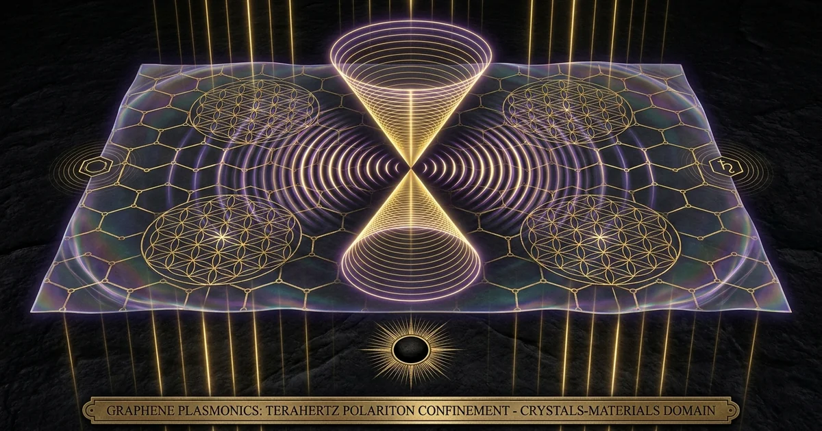
Graphene Plasmonics: Terahertz Polariton Confinement
Mineral Classification & Crystallographic Thesis
Allotropic Carbon Taxonomy and the Dirac Semimetal Matrix
Native carbon displays an allotropic spectrum unmatched in condensed matter physics, ranging from the three-dimensional $sp^3$-coordinated tetrahedral network of diamond (space group $Fd\bar{3}m$) to the layered planar arrays of graphite (space group $P6_3/mmc$). At the ultimate two-dimensional boundary of this taxonomy sits graphene: an isolated, single atom-thick sheet of carbon arranged in a honeycomb network belonging strictly to the dihexagonal dipyramidal plane group $p6mm$. Within this strictly planar crystal, carbon atoms form trivalent $\sigma$-bonds through overlapping $sp^2$ hybrid orbitals, yielding a carbon-carbon bond length of approximately $1.42\text{ \AA}$ and an in-plane Young’s modulus on the order of $1.0\text{ TPa}$. The remaining unhybridized $2p_z$ orbitals orient orthogonal to the basal plane, forming a delocalized, continuous $\pi$-electron network that dictates the low-energy electrodynamic phenomena of the crystal.
Crystal System: Two-Dimensional Hexagonal; Plane Group: $p6mm$ (Bulk Parent Graphite: $P6_3/mmc$).
In-Plane Carbon-Carbon Bond Length ($d_{\text{C-C}}$): $1.420 \pm 0.002\text{ \AA}$; Unit Cell Parameter ($a$): $2.461\text{ \AA}$.
Effective Mechanical Stiffness: $1.0\text{ TPa}$ equivalent bulk modulus; Breaking Strength: $42\text{ N/m}$.
Intrinsic Carrier Mobility ($\mu$): Exceeding $200,000\text{ cm}^2/(\text{V}\cdot\text{s})$ at $T = 300\text{ K}$ (suspended or encapsulated).
Dirac Velocity ($v_F$): $1.0 \times 10^6\text{ m/s}$; Charge Carrier Mass ($m^*$): Effectively zero at the $K$ and $K’$ Brillouin boundary points.
Primary Structural Baseline: Novoselov, K.S., Geim, A.K., et al. (2004) ‘Electric Field Effect in Atomically Thin Carbon Films’, Science, 306(5696), pp. 666–669.
When exfoliated to its pristine monoatomic boundary, the crystal ceases to behave as a conventional zero-gap semiconductor and instead instantiates an archetype of the two-dimensional dirac-semimetal. In this configuration, the electronic band structure exhibits linear energy-momentum dispersion at the corners of the first Brillouin zone. The point contacts between the conical valence ($\pi$) and conduction ($\pi^*$) bands—termed Dirac points ($K$ and $K’$)—impose conical energy manifolds described by a massless Dirac Hamiltonian rather than the standard parabolic Schrödinger equation. Consequently, low-energy charge carriers propagate through the planar crystal with an effective Fermi velocity $v_F \approx 10^6\text{ m/s}$, decoupled from the inertial mass constraints characteristic of standard three-dimensional metallurgical conductors.
The pristine sheet’s crystal symmetry prevents the spontaneous opening of a bandgap unless the inversion symmetry of the bipartite lattice is explicitly broken by foreign substrates, strain fields, or external chemical potentials. For investigative work in advanced mineral architectures, researchers reference /crystals-materials/graphite-lattice-dynamics to track how interlayer van der Waals bonding degrades the relativistic properties of isolated graphene into conventional bulk semimetallic bands. The preservation of this isolated $p6mm$ planar symmetry serves as the absolute baseline requirement for supporting massless charge carrier dynamics and the resulting coherent polaritonic fields.
Linear Dispersion and the Two-Dimensional Electron Gas Paradigm
The immediate physical consequence of the relativistic conical band structure is the formation of a two-dimensional-electron-gas characterized by an energy dispersion relationship $E(\mathbf{k}) = \hbar v_F |\mathbf{k}|$, where $\hbar$ denotes the reduced Planck constant and $\mathbf{k}$ represents the wavevector measured relative to the Dirac points. Unlike conventional semiconductor heterostructures (such as gallium arsenide or silicon inversion layers) where the two-dimensional-electron-gas is constrained by an effective electron mass $m^*$, the density of states in monolayer graphene vanishes linearly at the Dirac neutrality point:
$$D(E) = \frac{2 |E|}{\pi (\hbar v_F)^2}$$
This linear progression of the density of states ensures that the optical and electronic properties of the lattice remain continuously responsive to external electrostatic perturbation. The absolute Fermi level, or fermi-energy ($E_F$), can be swept symmetrically between the valence and conduction bands through the application of an external electrostatic gate field. This shifts the dominant carrier species between holes and electrons without modifying the parent carbon architecture.
Because the kinetic energy of the charge carriers scales linearly with momentum rather than quadratically, their thermodynamic and dielectric properties diverge from typical Fermi-liquid behaviors. The cyclotron mass is directly proportional to the square root of the carrier density:
$$m_c = \frac{E_F}{v_F^2} = \frac{\hbar \sqrt{\pi n}}{v_F}$$
This dynamic establishes an operational regime wherein high-density states do not suffer from the inertial damping seen in noble metals. At room temperature, the electron scattering rates remain bounded by intrinsic acoustic phonon interactions, yielding intrinsic mobilities that routinely exceed $200,000\text{ cm}^2/(\text{V}\cdot\text{s})$ when decoupled from extrinsic dielectric substrate noise.
Relativistic Dirac Cone (Linear: E = ħ v_F |k|)
       \       /   <-- Conduction Band (π*)
        \     /
         \   /
          \ /
           X       <-- Dirac Point (K, K') / Zero-Gap Neutrality
          / \
         /   \
        /     \
       /       \   <-- Valence Band (π)
The realization of such an unhindered two-dimensional-electron-gas within an exposed, atomically planar interface enables collective charge oscillations to couple directly with external transverse magnetic fields. The lack of an out-of-plane dimension confines screening currents exclusively to the $xy$-plane, intensifying Coulomb interactions among carriers. This structural framework transforms graphene from an inert crystallographic specimen into an active, field-responsive interface that underpins the physics of graphene plasmonics terahertz surface plasmon polaritons.
The Terahertz Polaritonic Thesis: Extreme Confinement Metrics
When electromagnetic radiation impinges upon the exposed carbon lattice, coupling between incident photons and the collective oscillations of the two-dimensional-electron-gas generates hybrid quasiparticles designated as a surface-plasmon-polariton (SPP). In traditional noble metals such as gold, silver, or copper, the bulk plasma frequency $\omega_p$ resides firmly in the ultraviolet spectral domain. Consequently, downconverting plasmonic resonances to infrared or terahertz frequencies requires the engineering of macroscopic sub-wavelength metamaterial geometries, which introduces severe ohmic damping losses and weak intrinsic field confinement.
In sharp contrast, graphene’s plasma frequency is fundamentally governed by its carrier density and scales directly with the Fermi energy:
$$\omega_p \propto \sqrt{\frac{e^2 E_F}{\epsilon_0 \epsilon_r \hbar^2}}$$
As established in foundational work by Koppens, Chang, and García de Abajo (2011), this functional dependence shifts the natural resonance of graphene surface plasmons into the mid-infrared, far-infrared, and terahertz spectral regimes ($0.1\text{ to }10\text{ THz}$, corresponding to free-space wavelengths $\lambda_0 \approx 30\text{ to }3000\text{ }\mu\text{m}$). In this domain, the kinetic inductance of the massless Dirac carriers becomes pronounced, compressing the polaritonic wavelength $\lambda_p$ to dimensions far smaller than the diffraction-limited free-space excitation wavelength.
Bulk Noble Metal (Gold/Silver):
  Plasma Frequency: Ultraviolet (Fixed, High Ohmic Loss in THz)
  Compression Factor: λ_0 / λ_p ≈ 1 to 5 (Weak THz Confinement)

Monolayer Graphene Matrix:
  Plasma Frequency: Mid-IR to THz (Continuously Gate-Tunable)
  Compression Factor: λ_0 / λ_p ≈ 50 to 200+ (Extreme Sub-Wavelength Confinement)
This phenomenon, defined as extreme sub-wavelength-confinement, routinely yields compression factors $\eta = \lambda_0 / \lambda_p$ exceeding two orders of magnitude ($\eta > 100$), confining terahertz electromagnetic energy into physical volumes that are a millionth of the free-space cubic wavelength ($\sim V_0 / 10^6$). The ability of an isolated $p6mm$ monoatomic carbon sheet to contract millimeter-scale electromagnetic radiation into nanometer-scale spatial profiles establishes graphene as a coherent transducer between ambient macro-scale fields and localized quantum mechanical systems. In-depth analysis of macroscopic devices leveraging this confinement can be found at /physics-electromagnetism/terahertz-metamaterials-field-confinement.
Lattice Geometry & Solid-State Physics
Honeycomb Lattice Topology and π-Band Orbital Overlap
The mechanical stability and electronic band topology of graphene emerge directly from the planar hexagonal arrangement of carbon atoms. The underlying Bravais lattice is hexagonal, defined by the primitive translation vectors:
$$\mathbf{a}_1 = \frac{a}{2}(3, \sqrt{3}), \quad \mathbf{a}_2 = \frac{a}{2}(3, -\sqrt{3})$$
where $a = 1.42\text{ \AA} \times \sqrt{3} \approx 2.46\text{ \AA}$ represents the lattice constant. Crucially, the honeycomb geometry is not a Bravais lattice in the strict mathematical sense; rather, it is a triangular Bravais lattice decorated with a two-atom basis, yielding two interpenetrating, chemically identical but crystallographically inequivalent triangular sublattices designated $A$ and $B$.
         (A)-------(B)
        /             \
       /   Sublattice  \
     (B)       A        (A)
       \               /
        \             /
         (A)-------(B)
         Lattice Constant a = 2.46 Å
         C-C Bond Length   d = 1.42 Å
Every carbon atom on sublattice $A$ is surrounded by three nearest-neighbor carbon atoms belonging to sublattice $B$, positioned along vectors:
$$\boldsymbol{\delta}_1 = \frac{a}{\sqrt{3}}\left(\frac{\sqrt{3}}{2}, \frac{1}{2}\right), \quad \boldsymbol{\delta}_2 = \frac{a}{\sqrt{3}}\left(-\frac{\sqrt{3}}{2}, \frac{1}{2}\right), \quad \boldsymbol{\delta}_3 = \frac{a}{\sqrt{3}}(0, -1)$$
This bipartite network forces an electron occupying the $2p_z$ orbital manifold to possess a two-component pseudospin wave function that characterizes the probability amplitude of the carrier residing on sublattice $A$ versus sublattice $B$. The geometric and spiritual ramifications of this dual-triangular hexagonal organization are analyzed in detail within /sacred-geometry/hexagonal-honeycomb-symmetries.
The overlap integral of the out-of-plane $2p_z$ orbitals produces the electronic transfer Hamiltonian. In a tight-binding framework, the energy bands take the analytical form:
$$E(\mathbf{k}) = \pm t \sqrt{3 + 2\cos(\mathbf{k}\cdot\mathbf{a}_1) + 2\cos(\mathbf{k}\cdot\mathbf{a}_2) + 2\cos(\mathbf{k}\cdot(\mathbf{a}_1 - \mathbf{a}_2))}$$
where $t \approx 2.8\text{ eV}$ represents the nearest-neighbor hopping energy. At the edges of the hexagonal Brillouin zone, located at the high-symmetry points:
$$\mathbf{K} = \left(\frac{2\pi}{3a}, \frac{2\pi}{3\sqrt{3}a}\right), \quad \mathbf{K}’ = \left(\frac{2\pi}{3a}, -\frac{2\pi}{3\sqrt{3}a}\right)$$
the energy term inside the radical vanishes identically, producing the zero-gap conical touching points.
An essential consequence of this two-sublattice topology is the generation of a non-trivial geometric phase—the Berry phase of $\pi$ acquired by a relativistic carrier completing an adiabatic closed path around the Dirac point. This $\pi$ phase shift induces destructive quantum interference between backscattering pathways when the scattering potential varies smoothly on the scale of the lattice constant, which dramatically suppresses backward electron scattering. This crystalline mechanism preserves ballistic charge transport and protects the coherent propagation of terahertz surface plasmon polaritons against scattering from long-range Coulomb impurities.
Dynamic Conductivity Formulations via the Kubo Formalism
The electromagnetic response of monolayer graphene to high-frequency transverse magnetic fields is dictated by its dynamic surface optical conductivity, $\sigma(\omega, E_F, \Gamma, T)$, where $\omega$ is the angular excitation frequency, $\Gamma$ is the phenomenological carrier scattering rate, and $T$ is the absolute thermodynamic temperature. Within the linear response regime and local limit ($q \to 0$), the conductivity is quantitatively governed by the random phase approximation using the local kubo-formula. This formulation separates the total conductivity tensor into additive intraband (Drude-like) and interband (quantum electronic transition) components:
$$\sigma(\omega) = \sigma_{\text{intra}}(\omega) + \sigma_{\text{inter}}(\omega)$$
The intraband contribution represents free-carrier collective acceleration within the Dirac cones and governs the lower spectral boundary encompassing the far-infrared and terahertz domains ($f \le 10\text{ THz}$):
$$\sigma_{\text{intra}}(\omega) = \frac{2i e^2 k_B T}{\pi \hbar^2 (\omega + i\Gamma)} \ln\left[2 \cosh\left(\frac{E_F}{2 k_B T}\right)\right]$$
In the degenerately doped degenerate limit where the chemical potential substantially exceeds the thermal energy ($|E_F| \gg k_B T$), this intraband expression simplifies into the canonical Drude model:
$$\sigma_{\text{intra}}(\omega) = \frac{i e^2 |E_F|}{\pi \hbar^2 (\omega + i\tau^{-1})}$$
where $\tau = \Gamma^{-1}$ signifies the carrier momentum relaxation lifetime. The imaginary component of $\sigma_{\text{intra}}$ is strictly positive, an absolute prerequisite for supporting transverse magnetic ™ surface-plasmon-polariton modes at a dielectric-graphene-dielectric interface.
Conversely, the interband conductivity accounts for quantum optical transitions of electrons hopping across the Dirac neutrality gap from the occupied lower Dirac cone into the empty upper Dirac cone:
$$\sigma_{\text{inter}}(\omega) = \frac{e^2}{4\hbar} \left[ G\left(\frac{\hbar\omega}{2}\right) + \frac{4i\hbar\omega}{\pi} \int_0^\infty \frac{G(\xi) - G(\hbar\omega/2)}{(\hbar\omega)^2 - 4\xi^2} d\xi \right]$$
where:
$$G(\xi) = \frac{\sinh(\xi / k_B T)}{\cosh(E_F / k_B T) + \cosh(\xi / k_B T)}$$
When the incident photon energy is less than twice the chemical potential ($\hbar\omega < 2|E_F|$), interband transitions are suppressed by pauli-blocking; all valence states with transition energies matching $\hbar\omega$ map directly to already-occupied states in the conduction cone. Thus, tuning the chemical potential above this threshold eliminates interband absorption, allowing terahertz polaritonic modes to propagate purely through the intraband regime without encountering catastrophic optical losses.
Dispersion Relations Governing Polariton Momentum Mismatch
The dispersion relation for transverse magnetic ™ surface plasmon polaritons guided by an infinitely thin, two-dimensional conducting sheet surrounded by two semi-infinite dielectric half-spaces with relative permittivities $\epsilon_1$ and $\epsilon_2$ is derived directly from Maxwell’s boundary conditions:
$$\frac{\epsilon_1}{k_{z1}} + \frac{\epsilon_2}{k_{z2}} + \frac{i\sigma(\omega)}{\omega \epsilon_0} = 0$$
where $\epsilon_0$ represents the vacuum permittivity, and $k_{zj} = \sqrt{k_p^2 - \epsilon_j k_0^2}$ designates the out-of-plane decay wavevector within the respective dielectric medium $j \in {1, 2}$, with $k_0 = \omega/c$ marking the free-space photon wavevector and $k_p$ representing the in-plane plasmon polariton wavevector.
In the non-retarded regime where the polariton momentum heavily exceeds the free-space photon momentum ($k_p \gg \sqrt{\epsilon_j} k_0$), the decay constants reduce to $k_{z1} \approx k_{z2} \approx k_p$. Under these boundary conditions, the explicit dispersion relation simplifies to:
$$k_p(\omega) \approx \epsilon_0 \frac{\epsilon_1 + \epsilon_2}{2} \frac{2i\omega}{\sigma(\omega)} = \frac{\pi \hbar^2 \epsilon_0 (\epsilon_1 + \epsilon_2)}{e^2 E_F} \omega(\omega + i\tau^{-1})$$
In the low-loss limit ($\omega \gg \tau^{-1}$), the real component of the polariton wavevector simplifies into a characteristic non-retarded square-law form:
$$q_{\text{real}} = \text{Re}(k_p) \approx \frac{\pi \hbar^2 \epsilon_0 (\epsilon_1 + \epsilon_2)}{e^2 E_F} \omega^2$$
Because $k_p$ is proportional to $\omega^2$ rather than the linear relationship $k_0 = \omega/c$ typical of free photons, the polariton wavevector is orders of magnitude larger than the free-space light vector at matching terahertz frequencies.
Wavevector Momentum Gap:
  k_0 = ω / c   (Free-space terahertz photon)
  k_p ∝ ω^2     (Graphene surface plasmon polariton)

  Since k_p >> k_0, momentum conservation prohibits direct light-to-plasmon conversion.
  A momentum matching mechanism is mandatory:
  k_p = k_0 sin(θ) + G, where G = 2π / Λ (Grating Period)
This momentum gap represents a substantial barrier: an incoming free-space terahertz photon cannot directly excite a graphene plasmon on an unpatterned sheet because energy and momentum cannot be simultaneously conserved. Overcoming this requires engineered momentum-matching architectures, such as metallic diffraction gratings, deep sub-wavelength dielectric waveguides, periodic nano-ribbon arrays, or the sharp tip of a near-field optical microscope.
By tailoring the spatial period $\Lambda$ of an array of periodic nano-ribbons, the effective spatial grating vector $G = 2\pi / \Lambda$ supplies the missing momentum $\Delta k$, permitting phase-matched transformation of macro-scale far-infrared fields into tightly bound polaritonic surface waves.
Subtle Energetic Dynamics & Resonance Mechanics
Dielectric Screening and Quantum Vacuum Fluctuations
Because monolayer graphene possesses no macroscopic vertical dimension, its surrounding dielectric environment directly establishes its electrostatic boundary conditions. The effective background dielectric constant experienced by the two-dimensional-electron-gas is governed by the arithmetic mean of its confining upper and lower substrates:
$$\epsilon_{\text{eff}} = \frac{\epsilon_{\text{super}} + \epsilon_{\text{sub}}}{2}$$
Any localized modification in the dielectric tensor of an adjacent medium—such as the deposition of a molecular monolayer, altered humidity gradients, or changes in biological substrate polarizability—directly shifts the polariton dispersion curve.
This sensitivity stems from the non-local dielectric screening mechanics inherent to low-dimensional materials. In three-dimensional bulk metals, large internal carrier densities screen field fluctuations over sub-angstrom Thomas-Fermi screening lengths, masking external dielectric shifts. In monolayer graphene, however, the in-plane dielectric screening function $\epsilon_{2D}(q, \omega)$ is bounded by the vanishing physical thickness of the carbon sheet:
$$\epsilon_{2D}(q, \omega) = 1 - v_q \Pi(q, \omega)$$
where $v_q = e^2 / (2 \epsilon_0 \epsilon_{\text{eff}} q)$ represents the two-dimensional Fourier-transformed Coulomb interaction and $\Pi(q, \omega)$ is the polarizability operator. The long-range nature of $v_q$ in two dimensions causes the local electric field to extend into the adjoining space, coupling localized quantum vacuum fluctuations directly to the moving surface charge carriers. The high spatial compression of the polaritonic mode concentrates the zero-point electromagnetic energy density, amplifying light-matter interactions and the spontaneous emission rates of neighboring quantum emitters via the Purcell effect.
Terahertz Polariton-Biofield Coherence and Collective Coupling
The terahertz operational window ($0.1\text{ to }10\text{ THz}$, or $3.3\text{ to }333\text{ cm}^{-1}$) is fundamentally aligned with the vibrational and rotational dynamics of biological macromolecules. The collective vibrational modes of cellular hydration shells, hydrogen-bond network librations in liquid water, the skeletal torsional dynamics of protein backbones, and the low-frequency conformational breathing of DNA helices all populate this spectral band.
When graphene plasmonics terahertz surface plasmon polaritons propagate along a bio-functionalized carbon interface, their evanescent fields extend into the adjacent biological medium over a distance dictated by the transverse decay wavevector:
$$\hat{z}_0 = \frac{1}{|k_z|} \approx \frac{1}{k_p} = \frac{\lambda_p}{2\pi}$$
Due to extreme sub-wavelength-confinement, this evanescent penetration depth scales down to tens of nanometers, matching the physical dimensions of cellular lipid bilayers, transmembrane ion channel proteins, and nucleic acid assemblies.
           EVANESCENT FIELD REGION (z ~ 10-50 nm)
  [ Biomembrane / Protein / Hydration Shell / Aqueous Layer ]
  ===========================================================
  [ MONOLAYER GRAPHENE LATTICE (p6mm Dirac Matrix)          ]
  -----------------------------------------------------------
  [ Dielectric Substrate (h-BN / SiO2 / Diamond)            ]
This spatial overlap facilitates coherent resonance between the graphene surface plasmons and the subtle dipolar oscillations of bio-organic molecules. Low, T., and Avouris, P. (2014) showed that when polaritonic modes match the natural vibrational frequencies of proximate molecular dipoles, the system enters a strong-coupling regime characterized by avoided crossings in polariton dispersion curves and the formation of hybrid plexcitonic states.
Rather than treating subtle biological fields as abstract or non-physical, modern electrodynamics conceptualizes the organismal biofield as a coherent, time-varying electromagnetic field generated by synchronized cellular dipolar oscillations, mitochondrial proton fluxes, and rhythmic ion channel gating. The graphene polaritonic sheet serves as a Phase-Locked loop detector and amplifier: non-thermal, low-intensity cellular terahertz signatures establish coherent phase-locking with the collective electron gas within the graphene lattice, converting elusive cellular electromagnetic dynamics into measurable, macroscopic electronic signals.
Nonlocal Hydrodynamic Effects and Subtle Energy Transduction
As the confinement factor $\lambda_0 / \lambda_p$ scales past 150, the polaritonic wavevector approaches the characteristic Fermi wavevector $k_F = \sqrt{\pi n}$ of the carrier gas, requiring corrections to the standard local Kubo conductivity model. In this compressed domain, nonlocal hydrodynamic interactions within the electron fluid become dominant:
$$\sigma_{\text{nonlocal}}(q, \omega) \approx \frac{\sigma_{\text{local}}(\omega)}{1 - \beta^2 q^2 / \omega(\omega + i\tau^{-1})}$$
where $\beta \approx \sqrt{3/4} v_F$ represents the hydrodynamic pressure velocity of the degenerate Dirac gas.
This nonlocal spatial dispersion prevents the polaritonic field from collapsing into an unphysical singularity. Instead, it generates a real-space quantum pressure gradient that redistributes the localized electron density across the $sp^2$ carbon lattice:
Nonlocal Hydrodynamic Boundary Action:
  Compressed THz Wavepacket (q -> k_F)
       │
       ▼
  [ Quantum Pressure Gradients (β^2 q^2) ]
       │
       ▼
  Modulates Differential Quantum Capacitance: C_Q = e^2 * D(E_F)
       │
       ▼
  Transduction of Minute Field Perturbations into Collective In-Plane Currents
This dynamic directly alters the sheet’s quantum capacitance:
$$C_Q = e^2 D(E_F) = \frac{2 e^2 \sqrt{n}}{\hbar v_F \sqrt{\pi}}$$
Because $C_Q$ acts in series with the geometric substrate capacitance $C_{\text{geom}}$, minute changes in external field potentials or subtle dielectric variations in adjacent organic matrices instantly modulate the overall capacitive state of the interface. Through this hydrodynamic coupling, graphene acts as an analog transducer, transforming ambient electromagnetic gradients and subtle energetic fluctuations into phase-coherent, in-plane charge-carrier modulations.
Noble Metals (Au / Ag)
- Operational Frequency: Strictly Ultraviolet to Visible ($\omega_p$ fixed by high bulk carrier density).
- Compression Metric ($\lambda_0 / \lambda_p$): Poor in THz band ($\approx 1\text{ to }5$).
- Dynamic Tunability: Inflexible. Carrier concentration is fixed crystallographically. Requires irreversible chemical or physical modification.
- Substrate Sensitivity: Confined to classical surface plasmon resonance (SPR) index shifts. Lacks atomic-scale sensitivity to subtle normal-mode vibrations.
- Damping Mechanics: Pronounced Drude ohmic losses at room temperature, driven by interband electron-phonon transitions.
Graphene ($p6mm$ Monolayer)
- Operational Frequency: Far-Infrared and Terahertz ($0.1\text{ to }10\text{ THz}$, matching molecular vibrations).
- Compression Metric ($\lambda_0 / \lambda_p$): Extreme sub-wavelength confinement ($\approx 50\text{ to }200+$).
- Dynamic Tunability: Dynamically gate-tunable via electrostatic field effect ($E_F$ swept from $-0.8\text{ to }+0.8\text{ eV}$).
- Substrate Sensitivity: Exceptional phase-space sensitivity; non-local quantum capacitance responds to single-dipole perturbations.
- Damping Mechanics: Minimal intraband damping when interband transitions are suppressed by Pauli-blocking ($2|E_F| > \hbar\omega$).
Historical Lapidary Lore & Traditional Lineage
The Mineralogical Ancestry of Plumbago and Graphite
Long before modern quantum electrodynamics revealed the Dirac semimetal nature of single-layer carbon, the macroscopic parent mineral graphite occupied an ambiguous niche in classical mineralogy. Renaissance and medieval lapidaries frequently misidentified the soft, lustrous carbonaceous mineral as an ore of lead or antimony, categorizing it under the umbrella terms plumbago or molybdaena. This classification arose from its metallic luster, low hardness (Mohs $1.0\text{ to }1.5$), and ability to leave a dark, cohesive mark upon parchment and slate.
Georgius Agricola, in his foundational metallurgical treatise De Re Metallica (1556), observed the presence of these soft, greasy, carbonaceous veins in Central European mines. Agricola noted that while the substance resembled lead ores (galena), it showed an anomalous resistance to heat, refusing to melt in conventional smelting crucibles where standard base metals readily liquefied.
Historical Mineral Classification:
  Ancient/Medieval: Plumbago / Molybdaena (Conflated with Lead/Antimony)
        │
  1556 (Agricola, De Re Metallica): Noted high-temperature refractory anomalies
        │
  1565 (Gesner, De Rerum Fossilium): First documentation of the lead-pencil insert
        │
  1779 (Scheele): Chemically identified as crystalline elemental carbon
        │
  1789 (Werner): Formally christened "Graphite" (Greek: γράφειν, "to write")
The mineral’s low friction and distinct tactile slip—macroscopic consequences of weak van der Waals bonding between atomically tough, planar sheets—drew the interest of early natural philosophers. They categorized plumbago as an earth mineral that defied the classical elemental dichotomies of combustible sulfur versus liquefiable mercury.
Agricola, G. (1556) De Re Metallica, Basel: Froben. Documents the anomalous refractory nature of carbonaceous plumbago ores across Bohemian mining tracts.
Gesner, C. (1565) De Rerum Fossilium Lapidum et Gemmarum Maxime Figuris & Similitudinibus, Zurich. Contains the earliest known morphological description of native graphite used for writing implements, noting its layered, slippery nature.
Theophrastus (c. 315 BCE) De Lapidibus. Classical descriptions of carbonaceous earths and mineral pigments possessing anomalous tactile properties.
Scheele, C.W. (1779) ‘Experiments on Plumbago’, Kongliga Vetenskaps Academiens Handlingar, pp. 238–245. The definitive chemical demonstration that plumbago consists of pure carbonized matter and nitric acid-resistant elemental carbon.
Conrad Gesner provided the first explicit documentation of encased writing graphite in his 1565 text De Rerum Fossilium, illustrating a wooden sleeve holding a shaped lead of plumbago mined from the historic Borrowdale deposit in Cumberland, England. Borrowdale yielded native graphite of unprecedented structural purity, allowing direct extraction of intact sheets and solid blocks. Miners and lapidaries observed that this material was chemically inert, resisted thermal stress, and preserved structural integrity under atmospheric exposure—qualities that made it vital for military applications, such as high-temperature crucibles for cannonballs, long before its electrical conductivity was recognized.
Alchemical Interpretations of the Carbonaceous Nigredo
Within historical hermetic and alchemical disciplines, raw carbonaceous matter occupied a revered conceptual station. Native graphite, representing dark, light-absorbing carbonaceous earth, was linked to the Nigredo (the Black Work)—the primordial baseline phase of the Magnum Opus. The Nigredo denoted the foundational stage: unstratified prime matter (prima materia) that carried the latent potential to yield the reflective clarity of the White Work (Albedo) and the ultimate transmutation into the philosopher’s stone.
Hermetic Alchemical Transmutation:
  [ Nigredo: Raw Plumbago / Black Earth ]
        │
        ▼ (Mechanical Shearing / Exfoliation)
  [ Albedo: Transparent Graphene Veil (2D Monolayer) ]
        │
        ▼ (Field Coupling / Electrostatic Gating)
  [ Rubedo: Coherent Terahertz Light-Matter Synthesis ]
Alchemists viewed this black carbon matrix not as an inert residue of combustion, but as an elemental base holding hidden, latent energy. The dense, opaque mineral concealed a hidden luminescence: the ability to structure, conduct, and direct subtle energetic currents. The tactile, lubricious feel of graphite was interpreted as a physical signature of internal fluidity, an indicator that the mineral remained internally dynamic despite its outward solid form.
This esoteric intuition closely mirrors the modern solid-state reality of the material. Bulk, light-absorbing graphite—the macroscopic embodiment of the Nigredo—is structurally transformed through the physical peeling of its basal planes. When reduced to a single, transparent two-dimensional veil, the opaque, inert carbonaceous mass becomes an optically transmissive matrix that guides, compresses, and amplifies invisible electromagnetic radiation across the terahertz spectrum. The transition from bulk graphite to monolayer graphene stands as a modern, laboratory realization of the classical transmutation: liberating trapped radiative potential from a dense, opaque mineral base.
Evolution from Renaissance Pigments to Monolayer Isolation
The path from utilizing Cumberland plumbago as a Renaissance marking implement to isolating individual carbon planes spanned centuries of material science. In 1789, the German mineralogist Abraham Gottlob Werner officially coined the term “graphite”—derived from the Greek verb graphein (“to write”)—formally separating the elemental carbon allotrope from metallic lead compounds. Soon after, Carl Wilhelm Scheele chemically proved that graphite was an allotrope of pure carbon by oxidizing it into carbon dioxide, confirming its elemental kinship to diamond.
By the mid-nineteenth century, chemists such as Benjamin Collins Brodie were actively investigating the chemical exfoliation of graphite. In 1859, Brodie exposed native graphite flakes to fuming nitric acid and potassium chlorate, successfully synthesizing graphite oxide. He observed that upon thermal shock, the intercalated carbon matrix expanded dramatically along its crystallographic $c$-axis, yielding ultrathin lamellae that hinted at the presence of single molecular sheets.
Theoretical investigations accelerated across the twentieth century. In 1947, P.R. Wallace published the first theoretical derivation of the electronic band structure of an isolated monoatomic carbon layer, treating it as an idealized mathematical model to calculate the optical and electronic properties of bulk graphite. Wallace recognized that the low-energy dispersions formed relativistic, linear cones at the Brillouin zone boundaries, but for decades the physical existence of isolated single-atom sheets was considered thermodynamically impossible at room temperature under the Peierls-Mermin theorem, which held that thermal fluctuations would destabilize any two-dimensional crystal.
This theoretical boundary stood until 2004, when Andre Geim and Kostya Novoselov at the University of Manchester achieved the mechanical exfoliation of monolayer graphene. Using adhesive polymer tape to strip basal layers from oriented pyrolytic graphite, they transferred single-layer sheets onto oxidized silicon substrates. Optical interference from the silicon dioxide layer made the single-atom carbon sheets visible under standard optical microscopy. This marked the practical synthesis of Wallace’s mathematical abstraction, unlocking direct empirical exploration of the massless Dirac semimetal and providing a reliable structural base for the development of graphene plasmonics terahertz surface plasmon polaritons.
Practical Applications, Calibration & Safety Protocols
Electrostatic Gating Architectures and Substrate Passivation
Activating graphene’s terahertz plasmonic modes requires precise electrostatic control over its chemical potential. In laboratory settings, this is achieved by integrating the exfoliated or chemically vapor-deposited (CVD) carbon monolayer into a field-effect transistor (FET) geometry. A highly doped silicon substrate typically functions as a macroscopic global backgate, separated from the graphene sheet by a thermally grown silicon dioxide ($\text{SiO}_2$) dielectric layer, typically $285\text{ to }300\text{ nm}$ thick:
Cross-Sectional Architecture of a Graphene THz Polaritonic Device:
  ============================================================
  [ S ] (Source Contact)           [ D ] (Drain Contact)
    │                                │
    └───> [ Graphene Monolayer (p6mm) ] <───┘
  ============================================================
  [ Hexagonal Boron Nitride (h-BN) Dielectric Spacer (5-20 nm) ]
  ------------------------------------------------------------
  [ Thermally Grown SiO2 Passivation Layer (285 nm)          ]
  ------------------------------------------------------------
  [ Heavily Doped Silicon Substrate (p++ Si Global Backgate)  ]
  ============================================================
                     │
                     └───> Gate Bias (V_g) -> Controls Fermi Level (E_F)
Applying a gate voltage $V_g$ relative to the source terminal alters the planar carrier density $n$ through the relation:
$$n = \frac{C_{\text{ox}}}{e} (V_g - V_{\text{CNP}})$$
where $C_{\text{ox}} = \epsilon_0 \epsilon_{\text{ox}} / d_{\text{ox}}$ is the gate oxide capacitance per unit area and $V_{\text{CNP}}$ represents the voltage at the charge neutrality point (the Dirac point).
Shifting $V_g$ alters the Fermi energy:
$$E_F = \hbar v_F \text{sgn}(n) \sqrt{\pi |n|}$$
sweeping the chemical potential symmetrically through the valence and conduction bands. This gating shifts the operational plasma frequency dynamically across the terahertz spectrum without structural modification.
However, direct deposition of pristine graphene onto standard $\text{SiO}_2$ exposes the electron gas to trap-state hysteresis, localized charge puddles, and optical phonon scattering from the amorphous substrate. To stabilize this interface, advanced polaritonic devices employ substrate passivation techniques: the oxide surface is chemically functionalized with self-assembled monolayers (SAMs) of hydrophobic molecules, such as hexamethyldisilazane (HMDS) or octadecyltrichlorosilane (OTS). This passivation layer eliminates dangling surface bonds and blocks adsorbed atmospheric water dipoles, suppressing parasitic charge trapping and extending polariton lifetimes.
Integration of Hexagonal Boron Nitride (h-BN) Dielectric Spacers
To realize long-range polariton propagation with minimal scattering losses, hexagonal-boron-nitride ($h$-BN) is the gold-standard dielectric substrate. Hexagonal boron nitride is an isomorph of graphene with a matching planar honeycomb structure ($a_{h\text{-BN}} = 2.50\text{ \AA}$, an in-plane lattice mismatch of less than $1.7%$). Unlike the semimetallic carbon lattice, however, the alternating boron and nitrogen sites break sublattice inversion symmetry, producing a wide bandgap insulator ($E_g \approx 5.9\text{ eV}$).
Hexagonal Boron Nitride (h-BN) Lattice Match:
  Graphene:  C - C  Bond Length = 1.42 Å | a = 2.46 Å
  h-BN:      B - N  Bond Length = 1.45 Å | a = 2.50 Å
  Lattice Mismatch < 1.7% -> Atomically Flat, Dangling-Bond-Free
Inserting an atomically smooth $h$-BN spacer between graphene and the underlying substrate provides critical physical advantages:
- Topographic Uniformity: Exfoliated $h$-BN flakes are free of surface dangling bonds and surface charge traps, reducing root-mean-square surface roughness to sub-angstrom scales ($R_q < 0.1\text{ nm}$). This prevents nanometer-scale conformational ripples that would otherwise scatter the two-dimensional-electron-gas.
- Mitigation of Localized Charge Puddles: The high dielectric quality of the underlying $h$-BN matrix suppresses inhomogeneous charge fluctuations, allowing the chemical potential to stay uniform across the entire sheet.
- Phonon-Polariton Synergy: Hexagonal boron nitride is a natural hyperbolic crystal that supports mid- to far-infrared optical phonon polaritons (Reststrahlen bands). Coupling graphene plasmons to these hyperbolic polaritons generates hybrid plasmon-phonon-polariton modes that propagate with extended lifetimes and heightened field confinement. Detailed fabrication and operational mechanics for these dielectric heterostructures are cataloged in /crystals-materials/hexagonal-boron-nitride-dielectrics.
Fully encapsulating monolayer graphene in an $h$-BN/Graphene/$h$-BN heterostructure shields the massless charge carriers from airborne chemical contamination, ambient water vapor, and substrate roughness. This architecture unlocks ballistic electron mean free paths exceeding $1\text{ }\mu\text{m}$ at room temperature, which sharply narrows the polaritonic resonance linewidths across the terahertz spectrum.
Material Toxicity, Inhalation Hazards, and Nano-Platelet Containment
While structurally integrated, substrate-bound graphene presents no significant exposure hazards, processing bulk-synthesized, powder-phase graphene nanoplatelets (GNPs) requires stringent safety measures. The physical features that give graphene its unique mechanical and electronic properties—sub-nanometer edge profiles, large specific surface area, and chemical stability—also pose meaningful biological and toxicological hazards when aerosolized.
Aerosolized graphene nanoplatelets (GNPs) pose severe biological and environmental hazards. Inhaled nanoplatelets bypass the protective mucosal filtration systems of the upper respiratory tract, depositing directly within the pulmonary alveoli. The sub-nanometer edges of structurally intact graphene flakes can mechanically impale and disrupt macrophage cell membranes, causing frustrated phagocytosis, unresolved oxidative stress, and progressive interstitial pulmonary fibrogenesis mimicking asbestiform pathology.
From a subtle energetic standpoint, inhaling structurally discontinuous carbon fragments introduces high-mobility conductive platelets into the respiratory tract. These platelets disrupt the endogenous terahertz vibrational coherence of epithelial tissue, inducing dielectric phase decoherence within the subtle biofield. Standard laboratory safety protocols dictate:
- No manipulation of dry, powdered graphene outside ISO Class 4 containment hoods.
- Mandatory use of certified, fit-tested HEPA/P100 respirators and anti-static containment boxes.
- Liquid-phase, bound polymer, or encased substrate-mounted configurations must be maintained at all processing stages to prevent airborne particulate release.
Toxicological studies demonstrate that the physical interaction of suspended graphene platelets with cellular architectures is governed by their lateral dimensions, layer thickness, and surface functionalization. Pristine, non-functionalized platelets resist enzymatic digestion; when ingested by alveolar macrophages, their sharp lateral geometries can trigger the mechanical rupture of phagolysosomes, causing the intracellular release of reactive oxygen species (ROS) and initiating pro-inflammatory cytokine cascades (e.g., IL-1$\beta$, TNF-$\alpha$).
Aerosol Exposure Pathway:
  Inhaled Dry Nanoplatelets
        │
        ▼
  Alveolar Deposition
        │
        ▼
  Macrophage Phagocytosis -> Mechanical Membrane Piercing (Sharp 2D Edges)
        │
        ▼
  Frustrated Phagocytosis & Lysosomal Rupture -> Intracellular ROS Release
        │
        ▼
  Chronic Interstitial Fibrosis & Biofield Dielectric Perturbation
To control these risks during device production:
- Synthesis via chemical vapor deposition (CVD) or micro-mechanical cleavage should always yield surface-bound monolayers or liquid-suspended phases.
- Sonication, centrifugation, and spray-coating of liquid-phase exfoliated graphene solutions must occur exclusively within certified chemical fume hoods with liquid containment traps.
- Sonication baths must be carefully sealed to prevent the emission of aerosols created by ultrasonic cavitation.
- Waste solutions containing suspended platelets must be handled as hazardous chemical waste, cross-linked into solid matrices prior to disposal to prevent carbon nanomaterials from entering the water table.
Frequently Asked Questions
How Does Tunable Fermi Energy Prevent Inherent Terahertz Loss?
The dynamic tunability of the fermi-energy ($E_F$) is the primary mechanism used to eliminate optical damping in graphene plasmonic architectures. When the chemical potential rests directly at the Dirac point ($E_F = 0\text{ eV}$), interband electronic transitions dominate. Under these conditions, an incoming photon with infinitesimal energy $\hbar\omega$ can promote an electron from the occupied lower Dirac cone into an empty state in the upper Dirac cone, creating an electron-hole pair that dissipates the electromagnetic energy into thermal phonons.
$$\text{Interband Absorption Threshold: } \hbar\omega > 2|E_F|$$
To suppress this loss mechanism, an electrostatic gate bias is applied to inject carriers, shifting the Fermi level away from the Dirac neutrality point:
Pauli-Blocking Mechanism:
       Conduction (π*)                Conduction (π*)
           \   /                          \===|===/   <-- Occupied up to E_F
            \ /                            \=====/
             X                              \===/     <-- Transitions Blocked
            / \                              / \          (Pauli Exclusion)
           /   \                            /   \
        Valence (π)                    Valence (π)
     E_F = 0 (Unblocked)            |E_F| > ħω / 2 (Pauli-Blocked)
  High Interband Absorption          Pure, Low-Loss Intraband Plasmons
Once the condition:
$$|E_F| > \frac{\hbar\omega}{2}$$
is achieved, pauli-blocking completely shuts down these optical transitions: all accessible electronic states within the conduction band up to energy $E_F$ are already occupied, and the Pauli exclusion principle prevents excitation into these populated states.
Because terahertz photon energies are extremely small ($1\text{ THz} \approx 4.14\text{ meV}$, requiring a modest gate shift of $|E_F| > 2.07\text{ meV}$), standard electrostatic gating easily drives the system into this blocked regime (routinely reaching $|E_F| \approx 200\text{ to }600\text{ meV}$). Under these operational conditions, interband absorption is entirely eliminated. The remaining optical loss is restricted to intraband Drude scattering from residual acoustic phonons and lattice impurities, allowing terahertz surface plasmon polaritons to propagate with exceptionally low damping.
What Differentiates Monolayer Graphene Polaritons from Bulk Graphite Plasmons?
The fundamental differences between monolayer graphene polaritons and bulk graphite plasmons stem from lattice dimensionality and electronic band structure:
Bulk Graphite Matrix:
  - Band Structure: Parabolic, 3D overlapping semimetallic bands.
  - Carrier Effective Mass: Finite inertial mass (m* > 0).
  - Out-of-Plane Screening: High vertical dielectric screening (ε_c ≈ 3-5).
  - Compression Metric: Low (λ_0 / λ_p ≈ 1 to 5).
  - In-Situ Tunability: None (Fixed carrier density n ~ 10^19 cm^-3).

Monolayer Graphene Matrix:
  - Band Structure: Linear, 2D relativistic Dirac cones (E = ħ v_F |k|).
  - Carrier Effective Mass: Massless Dirac fermions (m* = 0).
  - Out-of-Plane Screening: No vertical screening; localized exclusively to 2D plane.
  - Compression Metric: Extreme sub-wavelength confinement (λ_0 / λ_p > 100).
  - In-Situ Tunability: Dynamic electrostatic gate tunability (-0.8 to +0.8 eV).
In bulk graphite, individual atomic layers are coupled via interlayer van der Waals bonds along the $c$-axis. This interlayer coupling transforms the relativistic conical dispersion into traditional, parabolic semimetallic bands with a finite, non-zero effective carrier mass ($m^* > 0$). These overlapping bands generate a fixed three-dimensional carrier density on the order of $n \sim 10^{19}\text{ cm}^{-3}$ that cannot be substantially modulated by electrostatic gating, as external fields are screened out within the outermost few atomic layers. Furthermore, bulk graphite’s large out-of-plane dielectric constant ($\epsilon_c \approx 3\text{ to }5$) heavily screens collective charge fluctuations, which severely degrades the sub-wavelength compression factor.
In contrast, monolayer graphene is decoupled from out-of-plane electronic screening. Its carriers behave as massless Dirac fermions whose density of states vanishes at the Dirac point. This geometry allows external gate voltages to modulate the carrier density and shift the operational plasma frequency throughout the entire volume of the material. Crucially, confining the electron gas to a strictly two-dimensional boundary restricts kinetic screening currents to the basal plane. This intensifies Coulomb interactions and yields polariton compression factors $\lambda_0 / \lambda_p$ exceeding two orders of magnitude—a level of electromagnetic confinement unachievable in bulk graphite.
How Does Environmental Humidity Impact Terahertz Surface Plasmon Modes?
Atmospheric moisture and ambient humidity are major sources of damping and operational drift in unencapsulated graphene plasmonic devices. Because the carbon sheet is entirely surface with no protective bulk volume, water molecules readily adsorb onto its basal plane:
Atmospheric Contamination Pathways:
  Ambient Water Vapor (H2O Dipoles)
       │
       ▼
  Physisorbed Surface Layer & Trapped Interfacial Water
       │
       ▼
  Asymmetric Hole Doping (Shifts V_CNP to positive voltages)
       │
       ▼
  Terahertz Polariton Damping via Water Librational Coupling
This atmospheric water adsorption degrades polaritonic performance through three mechanisms:
- Extrinsic Hole-Doping and Neutrality Drift: Adsorbed water molecules act as electron acceptors, particularly in the presence of dissolved atmospheric trace gases like oxygen. This causes uncalibrated $p$-type doping, shifting the charge neutrality point ($V_{\text{CNP}}$) toward positive gate voltages and disrupting the electrostatic calibration of the system.
- Coupling to Water Librational Modes: Liquid water exhibits strong, broad absorption bands throughout the terahertz and far-infrared regions, driven by the collective relaxation and librational modes of its hydrogen-bonded network (most notably centered near $f \approx 1\text{ to }5\text{ THz}$). The evanescent tail of a graphene surface plasmon extends several tens of nanometers normal to the sheet, directly overlapping with these adsorbed water layers and inducing severe dielectric loss that broadens polaritonic resonances and shortens propagation distances.
- Dielectric Asymmetry and Carrier Scattering: Adsorbed water clusters form uneven dielectric islands on the surface. These islands scatter the two-dimensional-electron-gas, reducing the overall momentum relaxation time $\tau$ and accelerating intraband damping.
To ensure reproducible, low-loss operation, graphene devices operating in the terahertz spectrum must be passivated using atomically thin encapsulation (such as hexagonal boron nitride), coated with hydrophobic fluoropolymer top-layers, or measured within dry-nitrogen purged environments or vacuum cryostats.
Prior to initiating polaritonic experiments or gathering terahertz spectroscopic data, calibrate the operational state of the graphene field-effect matrix using this protocol:
- Environmental Evacuation & Thermal Degas: Mount the sample inside an environmental test chamber. Pump down to high vacuum ($P < 10^{-5}\text{ Torr}$) and bake at $T = 400\text{ K}$ for 120 minutes to thermally desorb physisorbed water molecules and volatile airborne hydrocarbons.
- Four-Point DC Conductivity Sweep: Connect the graphene device to a low-noise source-measure unit (SMU). While sourcing a stable $I_{ds} = 1\text{ }\mu\text{A}$ across the source and drain terminals, sweep the gate voltage $V_g$ symmetrically across the expected neutrality window (typically $-40\text{ V} \le V_g \le +40\text{ V}$ for standard $285\text{ nm }\text{SiO}2$ backgates). Record the channel resistance $R{xx}(V_g)$.
- Locate the Dirac Point ($V_{\text{CNP}}$): Identify the resistance peak $\max(R_{xx})$, which marks the Dirac charge neutrality point. A clean, un-doped device should exhibit $|V_{\text{CNP}}| \le 5\text{ V}$. If $V_{\text{CNP}} > +15\text{ V}$, residual $p$-doping is present, requiring an extended vacuum bake.
- Mobility Extraction via Field-Effect Model: Calculate the intrinsic field-effect mobility $\mu_{\text{FE}}$ from the linear transconductance regime: $$\mu_{\text{FE}} = \frac{L}{W \cdot C_{\text{ox}}} \left( \frac{\partial \sigma}{\partial V_g} \right)$$ Verify that $\mu_{\text{FE}} \ge 10,000\text{ cm}^2/(\text{V}\cdot\text{s})$ on passivated $\text{SiO}_2$ or $\ge 60,000\text{ cm}^2/(\text{V}\cdot\text{s})$ on encapsulated $h$-BN at room temperature before proceeding.
- THz-TDS Reference Transmission: Align a Terahertz Time-Domain Spectrometer (THz-TDS) to measure transmission through the active graphene channel. Set the gate bias to the target Fermi energy: $$V_g = V_{\text{CNP}} + \frac{e E_F^2}{\pi \hbar^2 v_F^2 C_{\text{ox}}}$$ Confirm that the characteristic polaritonic transmission dip appears at the calculated momentum-matched resonance frequency.
:::